,换一芯片,断开2路MOS的D极,接上外部Vdd,可观察到DRV1,DRV2均有脉冲输出(占空比很小,随输入AC反比,AC<71V时输出关断),接通MOS的D极,不能正常PFC工作,检测发现pin6(ss端,误差放大器基准)电压为1V左右,且随输入AC正比变化,是否IC已损坏?
 还是被内部mos嵌位?(从结构图上看,该端口与内部MOS相连)
另外一个问题:作为220V的线路,如何把欠压关断设定在175V(Rmot<40k会不会有问题?)
 各位老大,拜托了!
 ,换一芯片,断开2路MOS的D极,接上外部Vdd,可观察到DRV1,DRV2均有脉冲输出(占空比很小,随输入AC反比,AC<71V时输出关断),接通MOS的D极,不能正常PFC工作,检测发现pin6(ss端,误差放大器基准)电压为1V左右,且随输入AC正比变化,是否IC已损坏?还是被内部mos嵌位?(从结构图上看,该端口与内部MOS相连)
各位老大,拜托了!
,换一芯片,断开2路MOS的D极,接上外部Vdd,可观察到DRV1,DRV2均有脉冲输出(占空比很小,随输入AC反比,AC<71V时输出关断),接通MOS的D极,不能正常PFC工作,检测发现pin6(ss端,误差放大器基准)电压为1V左右,且随输入AC正比变化,是否IC已损坏?还是被内部mos嵌位?(从结构图上看,该端口与内部MOS相连)
各位老大,拜托了! 500) {this.resized=true; this.width=500; this.alt='这是一张缩略图,点击可放大。\n按住CTRL,滚动鼠标滚轮可自由缩放';this.style.cursor='hand'}" onclick="if(!this.resized) {return true;} else {window.open('http://u.dianyuan.com/bbs/u/83/2921441257588729.gif');}" onmousewheel="return imgzoom(this);">
 500) {this.resized=true; this.width=500; this.alt='这是一张缩略图,点击可放大。\n按住CTRL,滚动鼠标滚轮可自由缩放';this.style.cursor='hand'}" onclick="if(!this.resized) {return true;} else {window.open('http://u.dianyuan.com/bbs/u/83/2921441257817694.gif');}" onmousewheel="return imgzoom(this);">
 500) {this.resized=true; this.width=500; this.alt='这是一张缩略图,点击可放大。\n按住CTRL,滚动鼠标滚轮可自由缩放';this.style.cursor='hand'}" onclick="if(!this.resized) {return true;} else {window.open('http://u.dianyuan.com/bbs/u/83/2073861257817904.gif');}" onmousewheel="return imgzoom(this);">
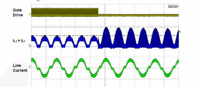 500) {this.resized=true; this.width=500; this.alt='这是一张缩略图,点击可放大。\n按住CTRL,滚动鼠标滚轮可自由缩放';this.style.cursor='hand'}" onclick="if(!this.resized) {return true;} else {window.open('http://u.dianyuan.com/bbs/u/83/2073861257820518.gif');}" onmousewheel="return imgzoom(this);">
 500) {this.resized=true; this.width=500; this.alt='这是一张缩略图,点击可放大。\n按住CTRL,滚动鼠标滚轮可自由缩放';this.style.cursor='hand'}" onclick="if(!this.resized) {return true;} else {window.open('http://u.dianyuan.com/bbs/u/83/2073861257820544.gif');}" onmousewheel="return imgzoom(this);">
 500) {this.resized=true; this.width=500; this.alt='这是一张缩略图,点击可放大。\n按住CTRL,滚动鼠标滚轮可自由缩放';this.style.cursor='hand'}" onclick="if(!this.resized) {return true;} else {window.open('http://u.dianyuan.com/bbs/u/83/2921441257907403.gif');}" onmousewheel="return imgzoom(this);">