【讨论】MOS驱动芯片的设计考虑
怎样根据MOS来选取合适的驱动芯片,芯片技术指标中那些与时间相关的参数到底有哪些影响,芯片内部的功耗如何计算,为什么把芯片的输入、或输出通过耦合电容、驱动变压器后波形存在了各种各样的问题,各种功率拓扑到底应该怎样设计驱动电路等.
全部回复(7)
正序查看
倒序查看
现在还没有回复呢,说说你的想法
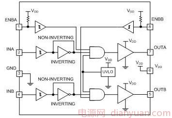
1。与时间相关的指标
1。1 上升与下降时间
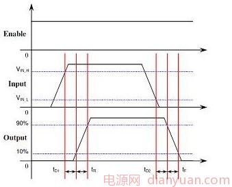
For the Rising time tr and Falling time tf are governed by three factors. These are operating temperature, supply voltage Vdd, and output load. Since the low side gate drivers were designed to drive power MOSFETs the output load is expressed in Farads. This is due to the fact that a MOSFET gate looks like a capacitor to the driving device, which is actually appears as a variable nonlinear capacitance. The rising time, tr, is defined as the period from 10% to 90% of output rail-to-rail level to supply source Vdd, while the falling time, tf, is defined as the period from 90% to 10% of output rail-to-rail level to supply source Vdd, both on Enable active, as shown in Fig. 1.
The rising and falling time is the function of output load Cload, supply voltage Vdd, and operating temperature. Little can be done to lower the rising and falling time except for keeping the device temperature low and choosing Cload as small as possible. There are several factors associated with the rising and falling times. In general, the rising and falling times are not equal creating a small asymmetry in the output waveform. This is due to having a P-channel device source current and an N-channel sink current from the load at the output stage. P-channels do not perform as well as N types, so this does not make the P equal to the N in dynamic performance. This difference is most obvious at higher loads. Meanwhile, rising and falling times also determine the minimum pulse width in that if an input pulse has a width that is less than the sum of the rising and falling times the output can’t make a full transition.
说白了,上升与下降时间是针对输出讲的,也就是驱动输出10%-90%之间的时间延迟。
0
回复
提示
@52football
1。与时间相关的指标1。1上升与下降时间FortheRisingtimetrandFallingtimetfaregovernedbythreefactors.Theseareoperatingtemperature,supplyvoltageVdd,andoutputload.SincethelowsidegatedriversweredesignedtodrivepowerMOSFETstheoutputloadisexpressedinFarads.ThisisduetothefactthataMOSFETgatelookslikeacapacitortothedrivingdevice,whichisactuallyappearsasavariablenonlinearcapacitance.Therisingtime,tr,isdefinedastheperiodfrom10%to90%ofoutputrail-to-railleveltosupplysourceVdd,whilethefallingtime,tf,isdefinedastheperiodfrom90%to10%ofoutputrail-to-railleveltosupplysourceVdd,bothonEnableactive,asshowninFig.1.TherisingandfallingtimeisthefunctionofoutputloadCload,supplyvoltageVdd,andoperatingtemperature.LittlecanbedonetolowertherisingandfallingtimeexceptforkeepingthedevicetemperaturelowandchoosingCloadassmallaspossible.Thereareseveralfactorsassociatedwiththerisingandfallingtimes.Ingeneral,therisingandfallingtimesarenotequalcreatingasmallasymmetryintheoutputwaveform.ThisisduetohavingaP-channeldevicesourcecurrentandanN-channelsinkcurrentfromtheloadattheoutputstage.P-channelsdonotperformaswellasNtypes,sothisdoesnotmakethePequaltotheNindynamicperformance.Thisdifferenceismostobviousathigherloads.Meanwhile,risingandfallingtimesalsodeterminetheminimumpulsewidthinthatifaninputpulsehasawidththatislessthanthesumoftherisingandfallingtimestheoutputcan’tmakeafulltransition.说白了,上升与下降时间是针对输出讲的,也就是驱动输出10%-90%之间的时间延迟。[图片]
顶!
继续~~~~学习中!
0
回复
提示
1。2 输入、输出延迟时间
The propagation delay could be cataloged as turn-on and turn-off delay times. The turn-on propagation delay from input to output, td1, is defined as the period from input high to 10% of output rail-to-rail level to supply source Vdd, while The turn-off propagation delay from input to output, td2, is defined as the period from input low to 90% of output rail-to-rail level to supply source Vdd, both on Enable active, as shown in Fig. 1. On the other hand, the enable on propagation delay from enable signal to output, td3, is defined as the period from Enable high to 10% of output rail-to-rail level to supply source Vdd, while the enable off propagation delay from enable signal to output, td4, is defined as the period from Enable low to 90% of output rail-to-rail level to supply source Vdd, both on input active, as shown in Fig.2
The propagation delay time is the function of input signal amplitude Vin, supply voltage Vdd, and operating temperature. Little can be done to lower the delay except for keeping the device temperature low. Need to note that slow rising input signals can give the appearance of long delay times. This comes from the fact that the trip point of the input (about 1.5V) of Schmitt trigger in the driver can often be higher than the 10% point in the waveform.
0
回复
提示
输入、输出的延迟指的是输入信号有、或无时,输出端对应的延迟时间。有时驱动芯片还有使能端,使能端的电平由高变低、或由低变高时,同样会造成输出驱动信号的延迟。输入、输出的信号传递延迟除了跟芯片内部设计相关以外,如果输入信号的上升沿、或下降沿过于平缓,也会引起传递时间变长。
可以把驱动芯片看作一个信号传输线,延迟时间为零当然最好。但是实际的芯片不可能做到延迟时间为零,因为芯片里面有一堆信号处理电路。这个延迟时间较长的坏处:闭环系统将存在延时,可能造成系统的不稳定;如果两个通道的驱动信号有一定的时序要求,可能会造成时序控制的混乱(该没的驱号可还有;该有的信号却无)。比如原边驱动与副边同步整流管一般要有延时,如果这个延时在某个时候失控了,就有可能造成炸管。
0
回复
提示