下面是Infineon 电源IC 大全
各位有空的时候进来看看
ICE X65系列1096126790.pdf
Infineon 电源IC 大全--+--各种电路拓扑!!!
全部回复(31)
正序查看
倒序查看
现在还没有回复呢,说说你的想法
PWM (Pulse Width Modulation) control ICs for SMPS
Highly efficient power supply controllers with low power stand-by and power factor correction (PFC) capabilities.1096127638.pdf1096127660.pdf
1096127712.pdf
1096127735.pdf1096127786.pdf1096127806.pdf1096127830.pdf1096127854.pdf
Highly efficient power supply controllers with low power stand-by and power factor correction (PFC) capabilities.1096127638.pdf1096127660.pdf
1096127712.pdf
1096127735.pdf1096127786.pdf1096127806.pdf1096127830.pdf1096127854.pdf
0
回复
提示
Power Combi (PWM+PFC) control IC for SMPS
IC including the PWM control for an SMPS and the control for the preconverter to improve the Power Factor and to reduce the harmonics of the AC input current.
1096128017.pdf
IC including the PWM control for an SMPS and the control for the preconverter to improve the Power Factor and to reduce the harmonics of the AC input current.
1096128017.pdf
0
回复
提示
PFC (Power Factor Correction) control ICs for SMPS
IC's for sinusoidal line current consumption.
Operating in discontinous mode to control boost converter as an active harmonic filter.
1096128248.pdf
1096128264.pdf
1096128326.pdf
1096128342.pdf
1096128355.pdf
IC's for sinusoidal line current consumption.
Operating in discontinous mode to control boost converter as an active harmonic filter.
1096128248.pdf
1096128264.pdf
1096128326.pdf
1096128342.pdf
1096128355.pdf
0
回复
提示
DC-DC
CoreControlTM- PWM Control ICs
PWM Contol ICs for high precision CPU core supplies
1096128825.pdf
1096128894.pdf
CoreControlTM- Gate Driver
Single/dual Gate Driver for efficient high-speed DC/DC buck converter designs
1096128963.pdf
1096128978.pdf
1096129001.pdf
1096129013.pdf
1096129029.pdf
CoreControlTM - Integrated Switch
Driver plus high-side and low-side MOSFET combined in a single package .
1096129148.pdf
0
回复
提示
Flyback Converter
INTRODUCTION:
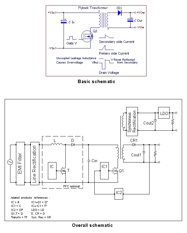
The Flyback converter is one of the simplest and most economical SMPS power supply topology, suited best to lower power levels, because the triangular current waveforms incur high peak losses in the primary side switch, and relatively high output ripple current and ripple voltage on the output side.
The flyback transformer is designed as an energy storage and transfer inductor, sized to store the energy required at the peak of the primary current during the first switching state. This maximum energy storage is irrespective of the input line voltage; variations in line voltage merely change the duty cycle required to charge the flyback transformer to the programmed current level. The transformer turns ratio is selected based on the allowable reflected flyback voltage as well as the desired output voltage. During the second switching state, the power switch must block the bus voltage « +Vin » plus the reflected reset voltage determined by the regulated «Vout» and the transformer turns ratio. Uncoupled inductance from the primary to secondary (leakage inductance) will also store energy, and since this energy is not clamped by the output winding, it will cause an avalanche on the primary unless clamped by an RCD snubber network.
BASICS OF OPERATION :
Energy transfer occurs by charging a current into the flyback inductor/transformer primary by turning on the power transistor. When the transistor turns off, the inductor reset on the secondary side conducts through CR1 to the output capacitor. Leakage inductance on the primary must be clamped on primary side (see below).
OVERALL SCHEMATIC
see global schematic below
 500) {this.resized=true; this.width=500; this.alt='这是一张缩略图,点击可放大。\n按住CTRL,滚动鼠标滚轮可自由缩放';this.style.cursor='hand'}" onclick="if(!this.resized) {return true;} else {window.open('http://u.dianyuan.com/bbs/u/21/1096129326.gif');}" onmousewheel="return imgzoom(this);">
 500) {this.resized=true; this.width=500; this.alt='这是一张缩略图,点击可放大。\n按住CTRL,滚动鼠标滚轮可自由缩放';this.style.cursor='hand'}" onclick="if(!this.resized) {return true;} else {window.open('http://u.dianyuan.com/bbs/u/21/1096129337.gif');}" onmousewheel="return imgzoom(this);">
INTRODUCTION:
The Flyback converter is one of the simplest and most economical SMPS power supply topology, suited best to lower power levels, because the triangular current waveforms incur high peak losses in the primary side switch, and relatively high output ripple current and ripple voltage on the output side.
The flyback transformer is designed as an energy storage and transfer inductor, sized to store the energy required at the peak of the primary current during the first switching state. This maximum energy storage is irrespective of the input line voltage; variations in line voltage merely change the duty cycle required to charge the flyback transformer to the programmed current level. The transformer turns ratio is selected based on the allowable reflected flyback voltage as well as the desired output voltage. During the second switching state, the power switch must block the bus voltage « +Vin » plus the reflected reset voltage determined by the regulated «Vout» and the transformer turns ratio. Uncoupled inductance from the primary to secondary (leakage inductance) will also store energy, and since this energy is not clamped by the output winding, it will cause an avalanche on the primary unless clamped by an RCD snubber network.
BASICS OF OPERATION :
Energy transfer occurs by charging a current into the flyback inductor/transformer primary by turning on the power transistor. When the transistor turns off, the inductor reset on the secondary side conducts through CR1 to the output capacitor. Leakage inductance on the primary must be clamped on primary side (see below).
OVERALL SCHEMATIC
see global schematic below
 500) {this.resized=true; this.width=500; this.alt='这是一张缩略图,点击可放大。\n按住CTRL,滚动鼠标滚轮可自由缩放';this.style.cursor='hand'}" onclick="if(!this.resized) {return true;} else {window.open('http://u.dianyuan.com/bbs/u/21/1096129326.gif');}" onmousewheel="return imgzoom(this);">
 500) {this.resized=true; this.width=500; this.alt='这是一张缩略图,点击可放大。\n按住CTRL,滚动鼠标滚轮可自由缩放';this.style.cursor='hand'}" onclick="if(!this.resized) {return true;} else {window.open('http://u.dianyuan.com/bbs/u/21/1096129337.gif');}" onmousewheel="return imgzoom(this);">
 0
回复
提示
@power-wang
FlybackConverter INTRODUCTION:TheFlybackconverterisoneofthesimplestandmosteconomicalSMPSpowersupplytopology,suitedbesttolowerpowerlevels,becausethetriangularcurrentwaveformsincurhighpeaklossesintheprimarysideswitch,andrelativelyhighoutputripplecurrentandripplevoltageontheoutputside.Theflybacktransformerisdesignedasanenergystorageandtransferinductor,sizedtostoretheenergyrequiredatthepeakoftheprimarycurrentduringthefirstswitchingstate.Thismaximumenergystorageisirrespectiveoftheinputlinevoltage;variationsinlinevoltagemerelychangethedutycyclerequiredtochargetheflybacktransformertotheprogrammedcurrentlevel.Thetransformerturnsratioisselectedbasedontheallowablereflectedflybackvoltageaswellasthedesiredoutputvoltage.Duringthesecondswitchingstate,thepowerswitchmustblockthebusvoltage«+Vin»plusthereflectedresetvoltagedeterminedbytheregulated«Vout»andthetransformerturnsratio.Uncoupledinductancefromtheprimarytosecondary(leakageinductance)willalsostoreenergy,andsincethisenergyisnotclampedbytheoutputwinding,itwillcauseanavalancheontheprimaryunlessclampedbyanRCDsnubbernetwork.BASICSOFOPERATION:Energytransferoccursbychargingacurrentintotheflybackinductor/transformerprimarybyturningonthepowertransistor.Whenthetransistorturnsoff,theinductorresetonthesecondarysideconductsthroughCR1totheoutputcapacitor.Leakageinductanceontheprimarymustbeclampedonprimaryside(seebelow).OVERALLSCHEMATICseeglobalschematicbelow[图片]500){this.resized=true;this.width=500;this.alt='这是一张缩略图,点击可放大。\n按住CTRL,滚动鼠标滚轮可自由缩放';this.style.cursor='hand'}"onclick="if(!this.resized){returntrue;}else{window.open('http://u.dianyuan.com/bbs/u/21/1096129326.gif');}"onmousewheel="returnimgzoom(this);">[图片]500){this.resized=true;this.width=500;this.alt='这是一张缩略图,点击可放大。\n按住CTRL,滚动鼠标滚轮可自由缩放';this.style.cursor='hand'}"onclick="if(!this.resized){returntrue;}else{window.open('http://u.dianyuan.com/bbs/u/21/1096129337.gif');}"onmousewheel="returnimgzoom(this);">
Two transistor Forward Converter
INTRODUCTION:
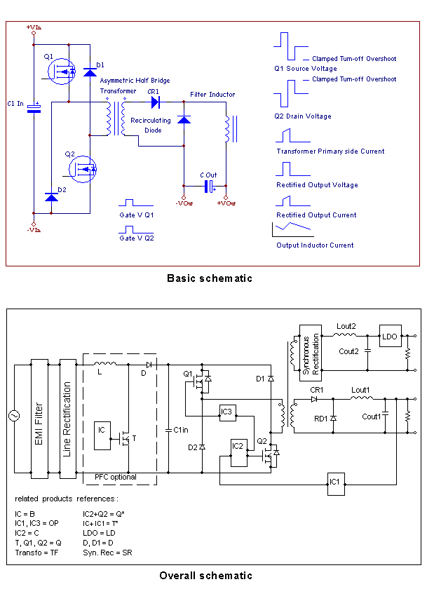
This SMPS topology has been widely used because of its robustness, simplicity, and moderately high performance. It is similar in performance characteristics to the single transistor forward converter, excepting that the two-transistor topology is inherently self-clamping for the magnetizing current reset of the power transformer, making avalanche operation unlikely. Additionally, this topology requires power transistors with only 1/2 the VDS blocking capability of the single transistor version. This reduction in voltage requirements dramatically reduces the RDS[on] for silicon area in the case of conventional MOSFET transistors, with the result that the two smaller transistors usually cost less than the single larger transistor, with lower total losses.
The two transistor forward converter is compatible with current mode control, and with the improved operating conditions for the transistor switches due to the lower operating voltage requirements, gives good performance in midrange power applications.
BASICS OF OPERATION :
Energy transfer occurs across the isolation transformer, when the power transistors Q1 and Q2 turn on, and the primary voltage is reflected across the output windings, and rectified by CR1, charging the output inductor. When the primary switch turns off, the flyback from the leakage inductance and magnetizing inductance flows through the clamp diodes D1 and D2, clamping the flyback of the primary and returning the energy from the magnetizing inductance of the transformer to the primary power bus (C1 In). The output inductor and output capacitor store energy and integrate the duty cycle so that the output voltage is proportional to the product of the rectified output voltage and duty cycle(see below).
 500) {this.resized=true; this.width=500; this.alt='这是一张缩略图,点击可放大。\n按住CTRL,滚动鼠标滚轮可自由缩放';this.style.cursor='hand'}" onclick="if(!this.resized) {return true;} else {window.open('http://u.dianyuan.com/bbs/u/21/1096129585.gif');}" onmousewheel="return imgzoom(this);">
 500) {this.resized=true; this.width=500; this.alt='这是一张缩略图,点击可放大。\n按住CTRL,滚动鼠标滚轮可自由缩放';this.style.cursor='hand'}" onclick="if(!this.resized) {return true;} else {window.open('http://u.dianyuan.com/bbs/u/21/1096129776.gif');}" onmousewheel="return imgzoom(this);">
INTRODUCTION:
This SMPS topology has been widely used because of its robustness, simplicity, and moderately high performance. It is similar in performance characteristics to the single transistor forward converter, excepting that the two-transistor topology is inherently self-clamping for the magnetizing current reset of the power transformer, making avalanche operation unlikely. Additionally, this topology requires power transistors with only 1/2 the VDS blocking capability of the single transistor version. This reduction in voltage requirements dramatically reduces the RDS[on] for silicon area in the case of conventional MOSFET transistors, with the result that the two smaller transistors usually cost less than the single larger transistor, with lower total losses.
The two transistor forward converter is compatible with current mode control, and with the improved operating conditions for the transistor switches due to the lower operating voltage requirements, gives good performance in midrange power applications.
BASICS OF OPERATION :
Energy transfer occurs across the isolation transformer, when the power transistors Q1 and Q2 turn on, and the primary voltage is reflected across the output windings, and rectified by CR1, charging the output inductor. When the primary switch turns off, the flyback from the leakage inductance and magnetizing inductance flows through the clamp diodes D1 and D2, clamping the flyback of the primary and returning the energy from the magnetizing inductance of the transformer to the primary power bus (C1 In). The output inductor and output capacitor store energy and integrate the duty cycle so that the output voltage is proportional to the product of the rectified output voltage and duty cycle(see below).
 500) {this.resized=true; this.width=500; this.alt='这是一张缩略图,点击可放大。\n按住CTRL,滚动鼠标滚轮可自由缩放';this.style.cursor='hand'}" onclick="if(!this.resized) {return true;} else {window.open('http://u.dianyuan.com/bbs/u/21/1096129585.gif');}" onmousewheel="return imgzoom(this);">
 500) {this.resized=true; this.width=500; this.alt='这是一张缩略图,点击可放大。\n按住CTRL,滚动鼠标滚轮可自由缩放';this.style.cursor='hand'}" onclick="if(!this.resized) {return true;} else {window.open('http://u.dianyuan.com/bbs/u/21/1096129776.gif');}" onmousewheel="return imgzoom(this);">
 0
回复
提示
@power-wang
TwotransistorForwardConverter INTRODUCTION:ThisSMPStopologyhasbeenwidelyusedbecauseofitsrobustness,simplicity,andmoderatelyhighperformance.Itissimilarinperformancecharacteristicstothesingletransistorforwardconverter,exceptingthatthetwo-transistortopologyisinherentlyself-clampingforthemagnetizingcurrentresetofthepowertransformer,makingavalancheoperationunlikely.Additionally,thistopologyrequirespowertransistorswithonly1/2theVDSblockingcapabilityofthesingletransistorversion.ThisreductioninvoltagerequirementsdramaticallyreducestheRDS[on]forsiliconareainthecaseofconventionalMOSFETtransistors,withtheresultthatthetwosmallertransistorsusuallycostlessthanthesinglelargertransistor,withlowertotallosses.Thetwotransistorforwardconverteriscompatiblewithcurrentmodecontrol,andwiththeimprovedoperatingconditionsforthetransistorswitchesduetotheloweroperatingvoltagerequirements,givesgoodperformanceinmidrangepowerapplications.BASICSOFOPERATION:Energytransferoccursacrosstheisolationtransformer,whenthepowertransistorsQ1andQ2turnon,andtheprimaryvoltageisreflectedacrosstheoutputwindings,andrectifiedbyCR1,chargingtheoutputinductor.Whentheprimaryswitchturnsoff,theflybackfromtheleakageinductanceandmagnetizinginductanceflowsthroughtheclampdiodesD1andD2,clampingtheflybackoftheprimaryandreturningtheenergyfromthemagnetizinginductanceofthetransformertotheprimarypowerbus(C1In).Theoutputinductorandoutputcapacitorstoreenergyandintegratethedutycyclesothattheoutputvoltageisproportionaltotheproductoftherectifiedoutputvoltageanddutycycle(seebelow).[图片]500){this.resized=true;this.width=500;this.alt='这是一张缩略图,点击可放大。\n按住CTRL,滚动鼠标滚轮可自由缩放';this.style.cursor='hand'}"onclick="if(!this.resized){returntrue;}else{window.open('http://u.dianyuan.com/bbs/u/21/1096129585.gif');}"onmousewheel="returnimgzoom(this);">[图片]500){this.resized=true;this.width=500;this.alt='这是一张缩略图,点击可放大。\n按住CTRL,滚动鼠标滚轮可自由缩放';this.style.cursor='hand'}"onclick="if(!this.resized){returntrue;}else{window.open('http://u.dianyuan.com/bbs/u/21/1096129776.gif');}"onmousewheel="returnimgzoom(this);">
Single Forward Converter
INTRODUCTION:
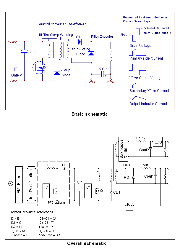
The single transistor forward converter offers some significant performance advantages compared to the flyback SMPS converter, but at the cost of many additional components. Instead of combining energy storage and voltage isolation/conversion in one magnetic component, a separate transformer and output filter inductor are used. They permit more favorable trapezoidal current waveforms and lower output current and voltage ripple, thus reducing noise and decreasing stress on semiconductors and capacitors. In a conventional scheme, the transformer reset occurs after the power transfer cycle, and requires that the input transistor blocks a minimum of twice the input voltage. For a maximum rectified bus voltage of 360V, a VDS rating of 800V is required for the power transistor Q1, unless alterations to the maximum duty cycle, and special clamp winding arrangements are made to lower the reflected voltage on Q1.
BASICS OF OPERATION :
Energy transfer occurs across the isolation transformer. When the power transistor Q1 turns on, the primary voltage is reflected across the output windings and then rectified by CR1, charging the output inductor. When the primary switch turns off, the bifilar primary clamp winding conducts through the clamp diode, clamping the drain voltage of Q1 at twice the input voltage, and returning the energy from the magnetizing inductance of the transformer to the primary power bus (C In). The driven side of the output inductor is clamped at 0.7 volts below ground by the recirculating diode. The output inductor and output capacitor store energy and integrate the duty cycle in such a manner that the output voltage is proportional to the product of the rectified output voltage and duty cycle (see frame below).
 500) {this.resized=true; this.width=500; this.alt='这是一张缩略图,点击可放大。\n按住CTRL,滚动鼠标滚轮可自由缩放';this.style.cursor='hand'}" onclick="if(!this.resized) {return true;} else {window.open('http://u.dianyuan.com/bbs/u/21/1096129929.gif');}" onmousewheel="return imgzoom(this);">
 500) {this.resized=true; this.width=500; this.alt='这是一张缩略图,点击可放大。\n按住CTRL,滚动鼠标滚轮可自由缩放';this.style.cursor='hand'}" onclick="if(!this.resized) {return true;} else {window.open('http://u.dianyuan.com/bbs/u/21/1096129939.gif');}" onmousewheel="return imgzoom(this);">
INTRODUCTION:
The single transistor forward converter offers some significant performance advantages compared to the flyback SMPS converter, but at the cost of many additional components. Instead of combining energy storage and voltage isolation/conversion in one magnetic component, a separate transformer and output filter inductor are used. They permit more favorable trapezoidal current waveforms and lower output current and voltage ripple, thus reducing noise and decreasing stress on semiconductors and capacitors. In a conventional scheme, the transformer reset occurs after the power transfer cycle, and requires that the input transistor blocks a minimum of twice the input voltage. For a maximum rectified bus voltage of 360V, a VDS rating of 800V is required for the power transistor Q1, unless alterations to the maximum duty cycle, and special clamp winding arrangements are made to lower the reflected voltage on Q1.
BASICS OF OPERATION :
Energy transfer occurs across the isolation transformer. When the power transistor Q1 turns on, the primary voltage is reflected across the output windings and then rectified by CR1, charging the output inductor. When the primary switch turns off, the bifilar primary clamp winding conducts through the clamp diode, clamping the drain voltage of Q1 at twice the input voltage, and returning the energy from the magnetizing inductance of the transformer to the primary power bus (C In). The driven side of the output inductor is clamped at 0.7 volts below ground by the recirculating diode. The output inductor and output capacitor store energy and integrate the duty cycle in such a manner that the output voltage is proportional to the product of the rectified output voltage and duty cycle (see frame below).
 500) {this.resized=true; this.width=500; this.alt='这是一张缩略图,点击可放大。\n按住CTRL,滚动鼠标滚轮可自由缩放';this.style.cursor='hand'}" onclick="if(!this.resized) {return true;} else {window.open('http://u.dianyuan.com/bbs/u/21/1096129929.gif');}" onmousewheel="return imgzoom(this);">
 500) {this.resized=true; this.width=500; this.alt='这是一张缩略图,点击可放大。\n按住CTRL,滚动鼠标滚轮可自由缩放';this.style.cursor='hand'}" onclick="if(!this.resized) {return true;} else {window.open('http://u.dianyuan.com/bbs/u/21/1096129939.gif');}" onmousewheel="return imgzoom(this);">
 0
回复
提示
@power-wang
SingleForwardConverter INTRODUCTION:ThesingletransistorforwardconverterofferssomesignificantperformanceadvantagescomparedtotheflybackSMPSconverter,butatthecostofmanyadditionalcomponents.Insteadofcombiningenergystorageandvoltageisolation/conversioninonemagneticcomponent,aseparatetransformerandoutputfilterinductorareused.Theypermitmorefavorabletrapezoidalcurrentwaveformsandloweroutputcurrentandvoltageripple,thusreducingnoiseanddecreasingstressonsemiconductorsandcapacitors.Inaconventionalscheme,thetransformerresetoccursafterthepowertransfercycle,andrequiresthattheinputtransistorblocksaminimumoftwicetheinputvoltage.Foramaximumrectifiedbusvoltageof360V,aVDSratingof800VisrequiredforthepowertransistorQ1,unlessalterationstothemaximumdutycycle,andspecialclampwindingarrangementsaremadetolowerthereflectedvoltageonQ1.BASICSOFOPERATION:Energytransferoccursacrosstheisolationtransformer.WhenthepowertransistorQ1turnson,theprimaryvoltageisreflectedacrosstheoutputwindingsandthenrectifiedbyCR1,chargingtheoutputinductor.Whentheprimaryswitchturnsoff,thebifilarprimaryclampwindingconductsthroughtheclampdiode,clampingthedrainvoltageofQ1attwicetheinputvoltage,andreturningtheenergyfromthemagnetizinginductanceofthetransformertotheprimarypowerbus(CIn).Thedrivensideoftheoutputinductorisclampedat0.7voltsbelowgroundbytherecirculatingdiode.Theoutputinductorandoutputcapacitorstoreenergyandintegratethedutycycleinsuchamannerthattheoutputvoltageisproportionaltotheproductoftherectifiedoutputvoltageanddutycycle(seeframebelow).[图片]500){this.resized=true;this.width=500;this.alt='这是一张缩略图,点击可放大。\n按住CTRL,滚动鼠标滚轮可自由缩放';this.style.cursor='hand'}"onclick="if(!this.resized){returntrue;}else{window.open('http://u.dianyuan.com/bbs/u/21/1096129929.gif');}"onmousewheel="returnimgzoom(this);">[图片]500){this.resized=true;this.width=500;this.alt='这是一张缩略图,点击可放大。\n按住CTRL,滚动鼠标滚轮可自由缩放';this.style.cursor='hand'}"onclick="if(!this.resized){returntrue;}else{window.open('http://u.dianyuan.com/bbs/u/21/1096129939.gif');}"onmousewheel="returnimgzoom(this);">
Half Bridge Converter
INTRODUCTION:
This converter design offers the possibility of reducing the size of the transformer by nearly 1/2 compared with the single transistor forward converter, because it's single ended push-pull configuration uses the transformer flux in both directions. It doesn't require a clamp winding, but does require two output windings, to support both polarities of output drive from the transformer. By replacing the small flux balance cap with a resonant network, it is possible to easily make a resonant mode converter, with very low switching losses because the voltage turn-on and turn-off occurs at very low current. The body diodes of the switching transistors Q1 and Q2 provide clamping of turn-off transients due to leakage inductance, so avalanche is not normally an issue with this topology.
BASICS OF OPERATION :
Energy transfer occurs across the isolation transformer, in single ended push-pull. First, when the power transistor Q1 turns on the primary voltage is reflected across the output windings, and rectified by CR1, charging the output inductor. When Q1 turns off, the voltage drive across the transformer primary drops to zero, and energy stored in the leakage and magnetizing inductances causes a turn-off overshoot, which is clamped by the body diode of Q2. In the second stage, Q2 turns on, and the transformer is driven in the opposite direction, resetting the flux balance in the transformer core. The output of the transformer is connected to a half wave rectifier, so the alternating polarity pulse train is rectified into a unidirectional pulse train of twice the frequency. The output capacitor and inductor store energy and integrate the duty cycle so that the output voltage is proportional to the product of the rectified output voltage and duty cycle (see below).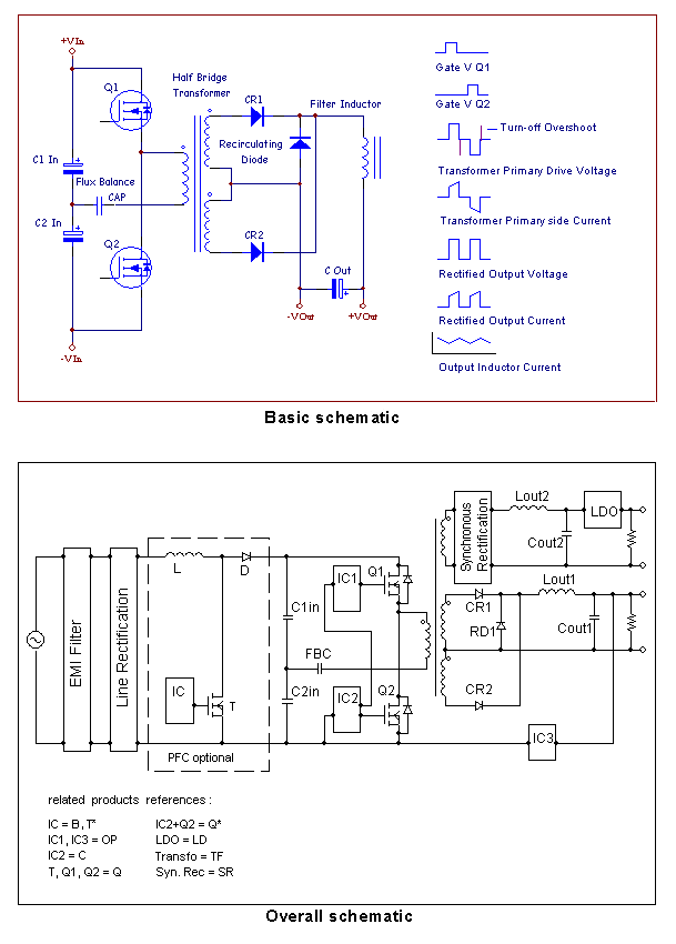 500) {this.resized=true; this.width=500; this.alt='这是一张缩略图,点击可放大。\n按住CTRL,滚动鼠标滚轮可自由缩放';this.style.cursor='hand'}" onclick="if(!this.resized) {return true;} else {window.open('http://u.dianyuan.com/bbs/u/21/1096130015.gif');}" onmousewheel="return imgzoom(this);">
 500) {this.resized=true; this.width=500; this.alt='这是一张缩略图,点击可放大。\n按住CTRL,滚动鼠标滚轮可自由缩放';this.style.cursor='hand'}" onclick="if(!this.resized) {return true;} else {window.open('http://u.dianyuan.com/bbs/u/21/1096130024.gif');}" onmousewheel="return imgzoom(this);">
INTRODUCTION:
This converter design offers the possibility of reducing the size of the transformer by nearly 1/2 compared with the single transistor forward converter, because it's single ended push-pull configuration uses the transformer flux in both directions. It doesn't require a clamp winding, but does require two output windings, to support both polarities of output drive from the transformer. By replacing the small flux balance cap with a resonant network, it is possible to easily make a resonant mode converter, with very low switching losses because the voltage turn-on and turn-off occurs at very low current. The body diodes of the switching transistors Q1 and Q2 provide clamping of turn-off transients due to leakage inductance, so avalanche is not normally an issue with this topology.
BASICS OF OPERATION :
Energy transfer occurs across the isolation transformer, in single ended push-pull. First, when the power transistor Q1 turns on the primary voltage is reflected across the output windings, and rectified by CR1, charging the output inductor. When Q1 turns off, the voltage drive across the transformer primary drops to zero, and energy stored in the leakage and magnetizing inductances causes a turn-off overshoot, which is clamped by the body diode of Q2. In the second stage, Q2 turns on, and the transformer is driven in the opposite direction, resetting the flux balance in the transformer core. The output of the transformer is connected to a half wave rectifier, so the alternating polarity pulse train is rectified into a unidirectional pulse train of twice the frequency. The output capacitor and inductor store energy and integrate the duty cycle so that the output voltage is proportional to the product of the rectified output voltage and duty cycle (see below).
 500) {this.resized=true; this.width=500; this.alt='这是一张缩略图,点击可放大。\n按住CTRL,滚动鼠标滚轮可自由缩放';this.style.cursor='hand'}" onclick="if(!this.resized) {return true;} else {window.open('http://u.dianyuan.com/bbs/u/21/1096130015.gif');}" onmousewheel="return imgzoom(this);">
 500) {this.resized=true; this.width=500; this.alt='这是一张缩略图,点击可放大。\n按住CTRL,滚动鼠标滚轮可自由缩放';this.style.cursor='hand'}" onclick="if(!this.resized) {return true;} else {window.open('http://u.dianyuan.com/bbs/u/21/1096130024.gif');}" onmousewheel="return imgzoom(this);">
 0
回复
提示
@power-wang
HalfBridgeConverter INTRODUCTION:Thisconverterdesignoffersthepossibilityofreducingthesizeofthetransformerbynearly1/2comparedwiththesingletransistorforwardconverter,becauseit'ssingleendedpush-pullconfigurationusesthetransformerfluxinbothdirections.Itdoesn'trequireaclampwinding,butdoesrequiretwooutputwindings,tosupportbothpolaritiesofoutputdrivefromthetransformer.Byreplacingthesmallfluxbalancecapwitharesonantnetwork,itispossibletoeasilymakearesonantmodeconverter,withverylowswitchinglossesbecausethevoltageturn-onandturn-offoccursatverylowcurrent.ThebodydiodesoftheswitchingtransistorsQ1andQ2provideclampingofturn-offtransientsduetoleakageinductance,soavalancheisnotnormallyanissuewiththistopology.BASICSOFOPERATION:Energytransferoccursacrosstheisolationtransformer,insingleendedpush-pull.First,whenthepowertransistorQ1turnsontheprimaryvoltageisreflectedacrosstheoutputwindings,andrectifiedbyCR1,chargingtheoutputinductor.WhenQ1turnsoff,thevoltagedriveacrossthetransformerprimarydropstozero,andenergystoredintheleakageandmagnetizinginductancescausesaturn-offovershoot,whichisclampedbythebodydiodeofQ2.Inthesecondstage,Q2turnson,andthetransformerisdrivenintheoppositedirection,resettingthefluxbalanceinthetransformercore.Theoutputofthetransformerisconnectedtoahalfwaverectifier,sothealternatingpolaritypulsetrainisrectifiedintoaunidirectionalpulsetrainoftwicethefrequency.Theoutputcapacitorandinductorstoreenergyandintegratethedutycyclesothattheoutputvoltageisproportionaltotheproductoftherectifiedoutputvoltageanddutycycle(seebelow).[图片]500){this.resized=true;this.width=500;this.alt='这是一张缩略图,点击可放大。\n按住CTRL,滚动鼠标滚轮可自由缩放';this.style.cursor='hand'}"onclick="if(!this.resized){returntrue;}else{window.open('http://u.dianyuan.com/bbs/u/21/1096130015.gif');}"onmousewheel="returnimgzoom(this);">[图片]500){this.resized=true;this.width=500;this.alt='这是一张缩略图,点击可放大。\n按住CTRL,滚动鼠标滚轮可自由缩放';this.style.cursor='hand'}"onclick="if(!this.resized){returntrue;}else{window.open('http://u.dianyuan.com/bbs/u/21/1096130024.gif');}"onmousewheel="returnimgzoom(this);">
Phase shifted ZVT Bridge Converter
INTRODUCTION:
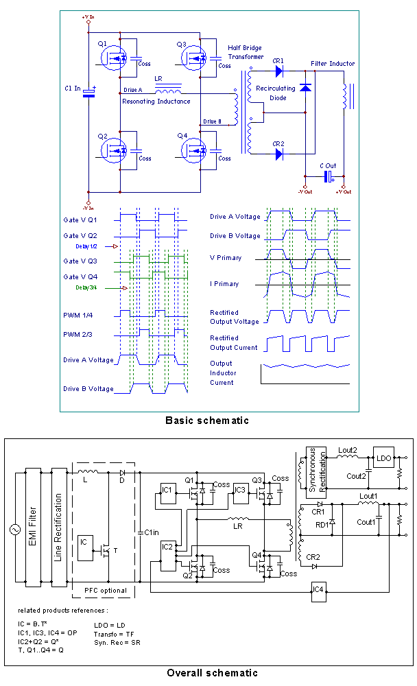
This topology presents a significant complexity compared to the conventional H Bridge because of the control scheme necessary to achieve Zero Voltage Transitions and essentially eliminate switching losses. Instead of using the simple anti-phase PWM modulation, unique timing signals are generated for each switching transistor, so that each side of the H bridge switches roughly in a square wave fashion at drive points A and B, and the displacement in phase between the square wave drives produces an effective PWM. The key advantage is that the drain to source transitions of each transistor are powered by the energy stored in the leakage inductance, or a primary resonant inductor. Each transistor turns on with 0V drain to source over a wide load range. The benefit lies in eliminating almost all of the switching losses of the MOSFET transistors, making possible increases in the operating frequency, reductions in the volume of the transformer and inductors.
BASICS OF OPERATION :
Energy transfer occurs across the isolation transformer in balanced push-pull. Key to the operation with no switching losses is the use of a phase shifted modulation scheme, using square waves on both sides of the transformer primary, and controlling the duty cycle across the transformer primary by changing the effective phase between the two square waves. To limit losses, drain to source transitions occur when one transistor in a leg turns off, and the inductance slews the drain to source voltage to the opposite potential, after which the other transistor is turned on. This requires the delays in switching control shown in Delay 1/2 and Delay 3/4, which shows in an exaggerated manner for clarity the timing delays required (see below).
 500) {this.resized=true; this.width=500; this.alt='这是一张缩略图,点击可放大。\n按住CTRL,滚动鼠标滚轮可自由缩放';this.style.cursor='hand'}" onclick="if(!this.resized) {return true;} else {window.open('http://u.dianyuan.com/bbs/u/21/1096130092.gif');}" onmousewheel="return imgzoom(this);">
 500) {this.resized=true; this.width=500; this.alt='这是一张缩略图,点击可放大。\n按住CTRL,滚动鼠标滚轮可自由缩放';this.style.cursor='hand'}" onclick="if(!this.resized) {return true;} else {window.open('http://u.dianyuan.com/bbs/u/21/1096130099.gif');}" onmousewheel="return imgzoom(this);">
INTRODUCTION:
This topology presents a significant complexity compared to the conventional H Bridge because of the control scheme necessary to achieve Zero Voltage Transitions and essentially eliminate switching losses. Instead of using the simple anti-phase PWM modulation, unique timing signals are generated for each switching transistor, so that each side of the H bridge switches roughly in a square wave fashion at drive points A and B, and the displacement in phase between the square wave drives produces an effective PWM. The key advantage is that the drain to source transitions of each transistor are powered by the energy stored in the leakage inductance, or a primary resonant inductor. Each transistor turns on with 0V drain to source over a wide load range. The benefit lies in eliminating almost all of the switching losses of the MOSFET transistors, making possible increases in the operating frequency, reductions in the volume of the transformer and inductors.
BASICS OF OPERATION :
Energy transfer occurs across the isolation transformer in balanced push-pull. Key to the operation with no switching losses is the use of a phase shifted modulation scheme, using square waves on both sides of the transformer primary, and controlling the duty cycle across the transformer primary by changing the effective phase between the two square waves. To limit losses, drain to source transitions occur when one transistor in a leg turns off, and the inductance slews the drain to source voltage to the opposite potential, after which the other transistor is turned on. This requires the delays in switching control shown in Delay 1/2 and Delay 3/4, which shows in an exaggerated manner for clarity the timing delays required (see below).
 500) {this.resized=true; this.width=500; this.alt='这是一张缩略图,点击可放大。\n按住CTRL,滚动鼠标滚轮可自由缩放';this.style.cursor='hand'}" onclick="if(!this.resized) {return true;} else {window.open('http://u.dianyuan.com/bbs/u/21/1096130092.gif');}" onmousewheel="return imgzoom(this);">
 500) {this.resized=true; this.width=500; this.alt='这是一张缩略图,点击可放大。\n按住CTRL,滚动鼠标滚轮可自由缩放';this.style.cursor='hand'}" onclick="if(!this.resized) {return true;} else {window.open('http://u.dianyuan.com/bbs/u/21/1096130099.gif');}" onmousewheel="return imgzoom(this);">
 0
回复
提示

