今天用磁环做了一个开环的隔离DC-DC.效果很差帮忙分析一下.样品的示意图和波形都有,另外一个是我自己做的那一个.
500) {this.resized=true; this.width=500; this.alt='这是一张缩略图,点击可放大。\n按住CTRL,滚动鼠标滚轮可自由缩放';this.style.cursor='hand'}" onclick="if(!this.resized) {return true;} else {window.open('http://u.dianyuan.com/bbs/u/75/2421751237814178.gif');}" onmousewheel="return imgzoom(this);">
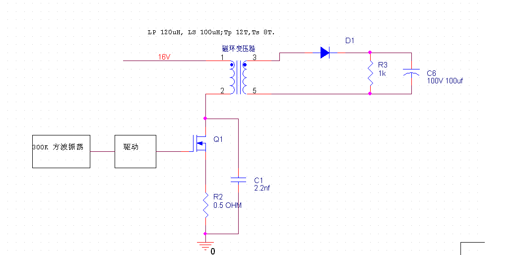
上图为样品的原理图.功率大概在2.5W左右.
500) {this.resized=true; this.width=500; this.alt='这是一张缩略图,点击可放大。\n按住CTRL,滚动鼠标滚轮可自由缩放';this.style.cursor='hand'}" onclick="if(!this.resized) {return true;} else {window.open('http://u.dianyuan.com/bbs/u/75/2421751237813930.gif');}" onmousewheel="return imgzoom(this);">
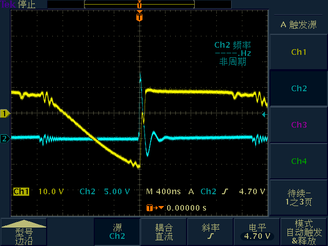
这个是样品的波形图.蓝色的是MOSFET D极的波形,黄色的是变压器副边的波形.
500) {this.resized=true; this.width=500; this.alt='这是一张缩略图,点击可放大。\n按住CTRL,滚动鼠标滚轮可自由缩放';this.style.cursor='hand'}" onclick="if(!this.resized) {return true;} else {window.open('http://u.dianyuan.com/bbs/u/75/2421751237814447.gif');}" onmousewheel="return imgzoom(this);">
这个是我自己做的东东.
波形很丑,是检流电阻的波形和变压器副边的波形,另一张是放大后的波形.500) {this.resized=true; this.width=500; this.alt='这是一张缩略图,点击可放大。\n按住CTRL,滚动鼠标滚轮可自由缩放';this.style.cursor='hand'}" onclick="if(!this.resized) {return true;} else {window.open('http://u.dianyuan.com/bbs/u/75/2421751237814540.gif');}" onmousewheel="return imgzoom(this);">
500) {this.resized=true; this.width=500; this.alt='这是一张缩略图,点击可放大。\n按住CTRL,滚动鼠标滚轮可自由缩放';this.style.cursor='hand'}" onclick="if(!this.resized) {return true;} else {window.open('http://u.dianyuan.com/bbs/u/75/2421751237814576.gif');}" onmousewheel="return imgzoom(this);">
这个波形里面可以看的到,在MOSFET刚开始导通的时候,检流电阻的波形上有一个很大尖峰.怎么弄都把那个尖峰去不掉.功耗很大,输入10V,电流有200mA.
反激电压有很高,加了去磁绕组的.
大侠们帮忙分析一下,要做到上面样品那样的波形,我该怎么做啊?这面很欠缺,望指教.